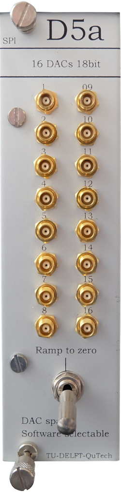
D5a - 16 Channel DAC
Description
The D5a module contains 16 18-bit DACs (Digital to Analog Converters), initially created for setting gate-voltages on samples. In contrast to most commercial units, there are no processor or clock circuits present in this module. This to prevent interference. The only time any digital signals are present is when the DAC values are being changed. Afterwards the module goes back to being static. The DAC values are set via the controller module. As this module is generally used for gate voltage control, the use of an isolated controller module (C1b/C2 combination) is recommended.
The output voltage range can be set via software. These ranges are: ±4V, ±2V, +4V, ±8V and +8V. Use of the ‘high’ voltage mode (±8V and ) requires an additional power supply. Whatever the voltage range setting, the DAC resolution is always 18-bit. This allows the user to choose the optimal range, without sacrificing resolution.

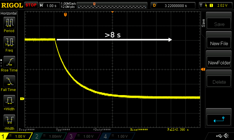
Above is a block diagram of the inner workings of the module. There are 16 DACs that have a shared internal reference, selected for low temperature drift and low noise. In between the DACs and the reference is the circuit responsible for the emergency switch: ramping the voltage up and down slowly. This can be used in a power outage where the computer is down but the output voltages need to be ramped down slowly. It ramps all the DACs up or down in 5 to 10 seconds. When the switch gets turned back on, the DACs will return smoothly to the previously set value. The emergency switch has a mechanical (pull lever before operating) lock to prevent accidental switching. Ramp down time measurement:
Summing Option
To increase the resolution it is possible to sum up two neighbouring DACs, at the expense of halving the total number of DACs. This is a small hardware modification for which the unit needs to be modified. The figure below shows an example of the summing option. Here two neighbouring channels have been added, with the second channel attenuated by a factor hundred. Both are kept at ±4V span, which results in LSB steps of 300nV. However, this is below the noise of the output. The measurement has been done by taking the average of 400 of these traces.
The typical use case for this option is to set one DAC (the course DAC) at a wanted value, and the vary the other DAC (the fine DAC) around that value. In this use case the linearity is not an issue. It also has the added effect that any glitches due to updating the DAC are also divided by the factor hundred.
Specifications
| Parameter | Value | Units | Conditions |
|---|---|---|---|
| Output Characteristics | |||
| Range | ±4, ±2, +4, (±8, +8) | V | ±8V and +8V only possible with additional power supply |
| Output Impedance | 550 | Ω | |
| Analog Bandwidth | 100 | kHz | Due to output filter |
| Maximum Update Rate | 5 | kSps | With data stream from PC |
| 250 | kSps | With data stream from controller module. Not yet implemented. | |
| Static Performance | |||
| Resolution | 18 | bit | |
| Monotonicity | 18 | bit | |
| DNL | ±0.2 | LSB | Typical value |
| INL | ±0.5 | LSB | Typical value |
| Dynamic Performance | |||
| Slew Rate | 1.4 | V/μs | |
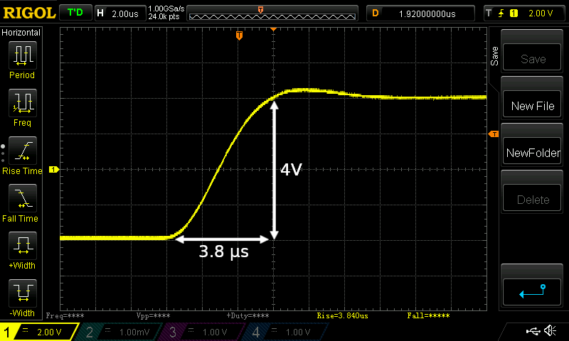
| Rise/Fall Time | 3.8 | μs | 10% to 90% |
| Overshoot | 4% | ||
| Integrated Noise | 0.5 | μVrms | 0.1 to 10 Hz bandwidth. |
| 9.5 | μVrms | 10 Hz to 100 kHz bandwidth. | |
| Wideband Noise Density | < 70 | nV/√Hz | @ 2 Hz |
| < 30 | nV/√Hz | @ 100 Hz | |
| Temperature Drift | 0.7ppm of range + 1.5ppm of output | ppm/°C | Preliminary measurement |
| Miscellaneous | |||
| Ramp up/down time | 5..10 | s | The safety switch ramp up/down time. |
| Supply Current | 100 | mA | |